Now Reading: India Embraces the Angstrom Era
-
01
India Embraces the Angstrom Era
Quick Summary
- The semiconductor industry is entering the “angstrom era,” where chip features are measured at the atomic scale, presenting new manufacturing challenges.
- Identifying and analyzing defects is more complex due to smaller chip features and advanced 3D architectures like FinFET and Gate-All-Around (GAA) transistors.
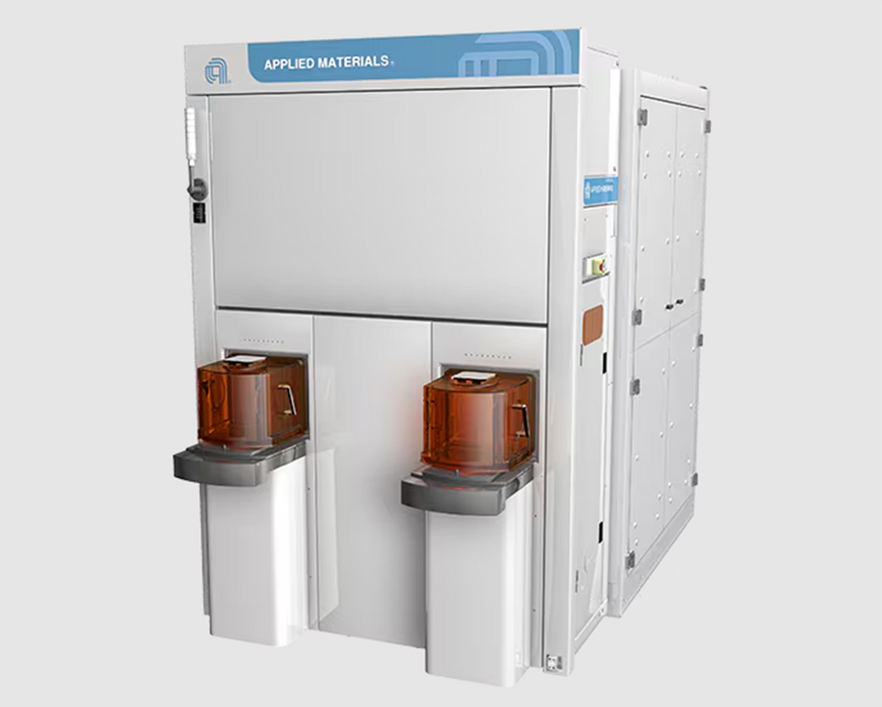
- Applied Materials has introduced Cold Field Emission (CFE) technology for electron beam (eBeam) systems, improving defect detection with sub-nanometer resolution and faster imaging speeds.
- CFE addresses limitations of previous technologies,such as system instability in lab environments caused by contaminants adhering to electron emitters at cold temperatures.
- AI-driven analytics are increasingly critical in defect classification, enabling engineers to distinguish between true defects and false alarms despite high data volumes.
- Applied Materials’ SEMVision H20 system combines second-generation CFE technology with deep learning AI models for accurate defect reviews at high throughput rates.
- These advancements aim to reduce cycle times, improve yields, lower costs of semiconductor production, and support emerging technologies like artificial intelligence (AI), autonomous vehicles, 5G connectivity.
images included:
- Defect map comparison during inspection – [Image Credit: Applied Materials]
- TFE vs. CFE electron emissions over a patterned surface – [Image Credit: Applied Materials]
- SEMVision H20’s imaging efficiency improvement chart – [Image Credit: Applied Materials]
Indian Opinion Analysis
the developments in semiconductor manufacturing described here reflect a pivotal moment for not only the global tech landscape but also India’s ambitions in electronics production. As one of the world’s fastest-growing consumer electronics markets-and home to goverment-led initiatives such as “Make in India”-advancements like cold Field Emission technology coudl catalyze innovation across domestic industries reliant on semiconductors.
Moreover, integrating artificial intelligence into defect detection aligns well with India’s expanding focus on AI research and its application across sectors like healthcare and transportation. While tools like SEMVision H20 emphasize precision critical for cutting-edge applications such as autonomous cars or advanced computing devices powered by AI algorithms globally-Indian manufacturers have an opportunity here to leverage similar technologies while scaling their capabilities.
The broader implication involves securing supply chains as demand-surging areas emerge (e.g., 5G infrastructure). As India works toward reducing dependency on imported chips through possible collaborations or production hubs catering export-consumption domestically optimistic signals trend regions pivot designing long-range alignment themselves competitors-production surmount smarter designs lasting outcomes competitive timelines


Related Posts


Stay Informed With the Latest & Most Important News
Previous Post
Next Post


Advertisement