

Now Reading: World’s First Room-Temperature Petahertz Phototransistor Unveiled
-
01
World’s First Room-Temperature Petahertz Phototransistor Unveiled
Fast Summary
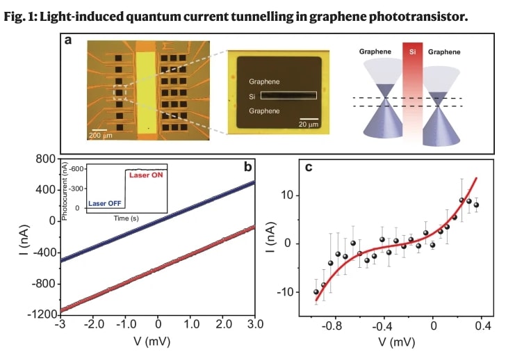
- Researchers demonstrated electron manipulation in graphene using light pulses lasting less than one quadrillionth of a second.
- This method leverages a quantum tunneling effect where electrons bypass barriers almost instantaneously, enabling potential processing speeds up to 1.6 petahertz (~638 attoseconds).
- Published findings in Nature Communications showcase advancements in ultrafast optoelectronic devices using graphene with tunable conductivity enhanced by laser parameters.
- Developed under ambient conditions, the graphene phototransistor combines light-induced currents (IL) and applied DC current for functionality as logic gates.
- The process offers breakthroughs toward petahertz optical transistors and future applications like quantum computing and ultrafast electronic switches.
- Researchers utilized modified commercially available graphene phototransistors to achieve this feat, paving the way for commercialization.
Image: !Graphene Phototransistor
Further Research: Achievements reflect years of work studying light-matter interaction through attosecond spectroscopy techniques to control electron motion at nanoscale levels.Significance: Sent data speeds could redefine customary computing and consumer electronics.Read More: Next Big Future Article
Indian Opinion Analysis
The progress of the world’s fastest petahertz-speed phototransistor represents a major milestone in global technological advancement with implications for India and also other nations working toward next-generation computing technologies. For India – which has prioritized sectors such as quantum research,semiconductor production,and AI-driven solutions – this scientific breakthrough provides both inspiration and opportunity.
The promise of ambient-condition capability means that commercial application could scale without relying on specialized lab setups or environmental constraints-an aspect meaningful for affordable integration into everyday devices globally, including emerging markets like India’s tech sector.
While there is no direct Indian involvement tied to these findings per se within the provided text context-it highlights critical areas where investment partnerships around applied physics expertise are viable collaboration jumping-off nodes bridging reliance/informal outsourcing pathways vs futuristic Trends scope leveraging mo쪽i


Related Posts


Stay Informed With the Latest & Most Important News
Previous Post
Next Post


Advertisement


