Now Reading: Semiconductor Breakthrough: Sub-10nm Era and 0.2nm Planar Transistors by 2039
-
01
Semiconductor Breakthrough: Sub-10nm Era and 0.2nm Planar Transistors by 2039
Quick Summary
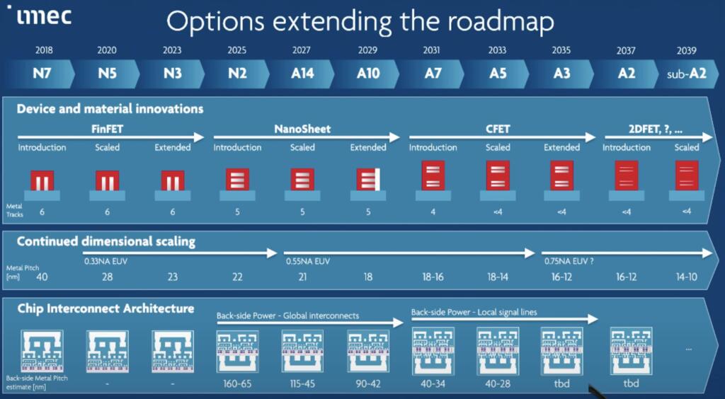
- IMEC, a leading research center in nanoelectronics and digital technologies, has released its Semiconductor Process Roadmap to 2039.
- The roadmap indicates a shift from size reduction to architectural innovation, moving from FinFET to NanoSheet and CFET to 2DFET transistor designs.
- Technological advancements required include EUV lithography upgrades (High NA EUV and Hyper NA EUV), backside power supply systems, and breakthroughs in materials like 2D semiconductors.
- Challenges outlined include quantum tunneling effects, manufacturing precision requirements for stacked architectures like CFETs, and material deposition techniques for atomic-level 2DFET processes.
- Hyper NA EUV technology aims for precision at scales below 10 nanometers with ASML pushing development toward atomic-scale manufacturing by leveraging advanced mirrors and optical systems.This technology faces hurdles such as cost escalation.
- Transition metal binary compounds are identified as promising materials for future transistors due to their manageable band gaps compared to graphene. Integration difficulties remain a barrier.
- IMEC predicts second-generation 2DFETs based on single-layer atomic materials will become mainstream by 2039 but notes advances will increase costs.
Images included:
- Semiconductor architecture evolution diagram
- High NA EUV roadmap illustration
- Deposition challenges visual guide
Indian Opinion Analysis
India’s aspirations in semiconductor manufacturing take on meaningful relevance with the technological shifts outlined by IMEC’s roadmap. Given India’s efforts through initiatives like the Semicon India program toward establishing production facilities alongside partnerships with global firms, advancements such as NanoSheet transistors or next-gen lithographic technologies present opportunities for fostering domestic R&D capabilities.
However, key challenges lie in catching up technologically; expertise required around CFET scaling or integrating two-dimensional semiconductors remains limited domestically compared to major players such as ASML or Tokyo Electron involved at these forefronts. Additionally, high costs associated with atomic-scale tooling may pose significant barriers unless robust government support is paired alongside investments.
If strategically prioritized through targeted skill-building programs or collaborations that marry India’s talent resource pool with international giants paving these advanced pathways-India could leverage these innovations not only for chip imports but eventual regional leadership roles across electronics ecosystems reliant directly foundational stability embracing dense chips summing “precision now vital edges ahead touch entire we ecosystem.” Optimistic timelines indicate importance ensuring efforts continuity bridging opportunity realization window finite tưởng possibilities tech generations.connection crucial


Related Posts


Stay Informed With the Latest & Most Important News
Previous Post
Next Post


Advertisement