Now Reading: Future of Semiconductors to 2039 – Finally Real Feature Sizes Under 10 Nanometers and 0.2 Nanometer Planar Transistor Equivalent
-
01
Future of Semiconductors to 2039 – Finally Real Feature Sizes Under 10 Nanometers and 0.2 Nanometer Planar Transistor Equivalent
Future of Semiconductors to 2039 – Finally Real Feature Sizes Under 10 Nanometers and 0.2 Nanometer Planar Transistor Equivalent
Imec is a world-leading research and innovation center in nanoelectronics and digital technologies. Imec has more than 6.000 employees and top researchers, for R&D in advanced semiconductor and system scaling, silicon photonics, artificial intelligence and more. They have been publishing semiconductor roadmaps. They are working with Tokyo Electron.
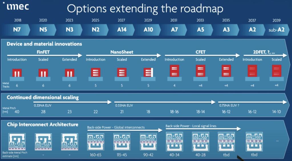
IMEC Releases Semiconductor Process Roadmap to 2039 and it cover NanoSheet and Lithography upgrades.
There was a paradigm shift in the semiconductor industry from size shrinkage to architectural innovation. The future will be a move from FinFET to NanoSheet, from CFET to 2DFET. Every transistor architecture innovation needs technological breakthroughs such as EUV lithography and backside power supply to keep improving chip density and performance.
However, the road ahead has never been easy. Quantum tunneling effect, 2D material preparation problems, ultra-precision lithography challenges, etc., all test the wisdom of the industry, requiring the industry to continue to breakthrough in equipment, materials and processes.
IMEC explains in detail how it predicts the trend and evolution of technologies such as chip process nodes, transistor architectures, chip interconnect architectures, backside power supply technologies, EUV lithography and 2D materials, as well as the difficulties and challenges in moving these technologies from the lab to industrialization.
The naming of the nodes does not correspond to actual physical dimensions anymore. It used to many nodes ago but does not now. Three-dimensional transistors dramatically increase transistor performance through a vertical stacking structure.
Today, the naming of chip process nodes is essentially a continuation of the equivalent planar transistor.


The End of the FinFET Era
The IMEC roadmap naming is not the TSMC, Samsung or Intel’s naming of process nodes.
Moving from N3 to N2, the transistor architecture has gradually evolved from FinFET (finned field effect tube transistor) to NanoSheet (nanosheet) transistor architecture.
Looking back at the development of semiconductor processes, for a long time in the past, it was the world of planar transistors.
Hyper NA EUV (0.75 NA), is Pushing Beyond Regular EUV
The fabrication of CFETs is not a straight path. CFET technology doubles the chip density of conventional architectures by vertically stacking N-type and P-type transistors, but it also poses challenges to the lithography process.
Inter-layer alignment for three-dimensional structures: The multi-layer stacked structure of CFETs requires sub-nanometer accuracy in the alignment of each layer’s pattern, and the high-resolution capability of Hyper NA EUV ensures precise interconnection of transistors between the different layers and reduces signal delays.
Etching requirements for high-density wiring: The metal interconnect layer spacing of CFET nodes is approaching 10 nanometers, and Hyper NA EUV, with its superior resolution, can form clearer circuit patterns on the photoresist, which, in combination with advanced etching technology, enables precise transfer of nanometer-scale wiring.
Getting the ultra-high precision and density manufacturing needs of CFETs, High NA EUV (0.55 NA) lithography is no longer able to meet the ultimate pursuit of precision, and Hyper NA EUV (0.75 NA) technology has emerged as a key tool to overcome the manufacturing challenges of CFETs. This technological pushes lithography precision to a new limit, but also marks the entry of semiconductor manufacturing processes into the era of atomic-level manipulation.
By increasing the numerical aperture (NA) to 0.75, Hyper NA EUV technology enables lithography systems to realize feature sizes approaching 10 nanometers, providing the necessary processing precision for the three-dimensional stacked architecture of CFETs.
ASML is developing a 0.75 NA Hyper NA EUV system with the goal of realizing 0.3nm node and below processes by 2035. There are huge technical hurdles, such as the need to fabricate meter-scale mirrors with atomic-level precision and the need to manage complex optical systems. The mirrors not only need to maintain higher precision, but also need to achieve complex beam regulation through precision drilling technology, which is an engineering marvel for the process challenge of “drilling atomic-scale holes in meter-scale lenses.
Jos Benschop, senior vice president of technology at ASML, has pointed out that while high numerical aperture and ultra-high numerical aperture technologies may continue Moore’s Law, physical limits such as quantum tunneling effects and atomic spacing may constrain technological progress until the middle of this century.
According to the roadmap disclosed by IMEC, a standard EUV lithography utilizing 0.3NA can support mass production up to the N2 node in 2025, and further down the line will need to be achieved through multiple exposure technology, but the A14, which will support mass production up to 2027, will be its limit.
The 0.55NA High NA EUV lithography can support the A5 process node until 2033. Further down the road, a 0.75NA Hyper NA EUV lithography may be necessary, perhaps to process nodes below A2 (0.2nm), where the roadmap has a question mark, so it’s not certain that Hyper NA EUV lithography will be able to support it.
2DFET
In the CFET era, the short channel effect still makes further miniaturization tricky again. As gate and channel lengths continue to shorten, semiconductor channels need to be made thinner and thinner to limit the channels through which current can flow and reduce the likelihood of carrier leakage when the device is turned off. If CFET devices are to be scaled to the A2 technology node so that the conducting channel lengths are reduced to less than 10 nm, then the silicon channel thickness must also be less than 10 nm. However, carrier mobility and device on-current are significantly reduced in such thin silicon channels.
2D semiconductors like transition metal sulfur compounds MX2, could be used. The IMEC roadmap shows that by 2037, when the process node evolves to A2, 2DFETs based on a single atomic layer of 2D material will replace CFET architectures with 0.75 NA EUV lithography, driving an exponential jump in chip density and performance.
2D materials provide unique advantages with their atomic-level thickness.
Potential for transition metal binary compounds: Materials such as tungsten disulfide (WS₂) and tungsten telluride (WTe₂) naturally form a single-molecule-layer crystalline structure, and their atomically-thin trench layers can boost gate capacitance to more than 10 times that of conventional silicon materials while suppressing leakage current. It is suitable for logic devices and high-frequency applications.
Limitations of graphene: Although graphene has excellent electrical conductivity, its zero bandgap characteristics make it impossible to realize the switching function of transistors, so 2DFET develops transition metal sulfides/tellurides with more focus on adjustable bandgap.
2DFET completely reconfigures the transistor operation by compressing the channel layer to a single atomic layer. Compared to the three-dimensional stacking architecture of CFETs, 2DFETs represent a “dimensional downgrade” innovation in semiconductor manufacturing: whereas CFETs rely on vertical stacking to increase density, 2DFETs achieve breakthroughs in performance through material dimensionality reduction, and the manufacturing process can be simplified by more than 30% (fewer deposition/etching steps).
Two-dimensional channel materials can bring significant performance gains at extremely miniaturized nodes, which has attracted the interest of major chip makers and academia. They have increased their investment in 2D materials R&D to overcome the hurdles of bringing 2D materials to the most advanced nodes.
IMEC expects second-generation 2DFETs based on 2D materials to become mainstream by 2039. However, the introduction of 2D materials still comes with a set of challenges that will increase the cost and integration difficulties when introducing them to A2 nodes.
IMEC also mentioned the following multi-faceted challenges and issues:
Deposition of 2D materials: First, it is a major challenge to form 2D material layers on wafers. For applications requiring high performance devices, there are two main routes:
(1) Growing 2D materials directly on the target substrate.
Direct growth typically requires a specific substrate and is performed at high temperatures (~1000°C). If industrially compatible processes and materials are required, this growth substrate may not be ideal and is not conducive to high crystallinity, which reduces film performance. However, direct growth may have the advantages of good uniformity, the ability to cover an entire wafer, and compatibility with industrial processes.

Brian Wang is a Futurist Thought Leader and a popular Science blogger with 1 million readers per month. His blog Nextbigfuture.com is ranked #1 Science News Blog. It covers many disruptive technology and trends including Space, Robotics, Artificial Intelligence, Medicine, Anti-aging Biotechnology, and Nanotechnology.
Known for identifying cutting edge technologies, he is currently a Co-Founder of a startup and fundraiser for high potential early-stage companies. He is the Head of Research for Allocations for deep technology investments and an Angel Investor at Space Angels.
A frequent speaker at corporations, he has been a TEDx speaker, a Singularity University speaker and guest at numerous interviews for radio and podcasts. He is open to public speaking and advising engagements.


Related Posts


Stay Informed With the Latest & Most Important News
Previous Post
Next Post


Advertisement