Now Reading: Laser Sail for Future Alpha Centauri Mission Now Costs $25 Million, Not $200 Billion
-
01
Laser Sail for Future Alpha Centauri Mission Now Costs $25 Million, Not $200 Billion
Laser Sail for Future Alpha Centauri Mission Now Costs $25 Million, Not $200 Billion
Laser pushed sails—ultrathin need reflective structures that are square meters but weight a gram. If the sails and the payload each weigh a gram, such a spacecraft could accelerate to one fifth of the speed of light. This would be 200 times faster than the Voyager probe. Richard Norte of Delft University of Technology, Netherlands, and his colleagues have demonstrated a nanometer-thick photonic-crystal material that could be used as the basis for the sails. They still need to make it about 4500 times larger than the sample that was produced. However, they have mass produced the nanoholes for the highly reflective but lightweight sails at 9000 times lower cost. This means a full size sail could be made for about 25 million euro. This cost breakthrough is key to actually making the sails. The method can be used for other movable lightweight mirrors.
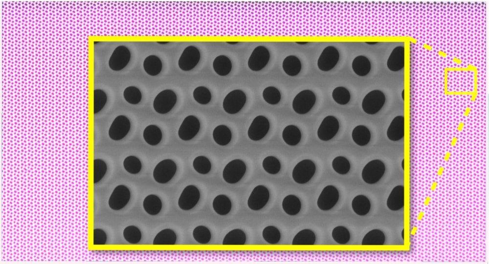
The researchers used a neural network to predict an optimal shape for the holes. The holes are oblong rather than circular. “It looks like a potato,” says Miguel Bessa of Brown University, Rhode Island, who led the theory side of the project. Specifically, the team arranged several potato shapes in a repeating five-neighbor pattern, or pentagonal lattice. The potato-shaped arrangement allows the system to respond to a broader range of wavelengths without having to make it thicker and thus heavier.
The Starshot Breakthrough Initiative aims to send gram-scale microchip probes to Alpha Centauri within 20 years, propelled by laser-driven lightsails at a fifth of light speed. This mission demands innovative lightsail materials with meter-scale dimensions, nanoscale thickness, and billions of nanoscale holes for enhanced reflectivity and reduced mass. Unlike the microchip payload, lightsail fabrication requires breakthroughs in optics, materials science, and structural engineering. Our study uses neural topology optimization, revealing a novel pentagonal lattice-based photonic crystal (PhC) reflector. The optimized designs significantly lower the acceleration times and, thereby, launch cost. Crucially, they also enabled orders-of-magnitude fabrication cost reduction. They made a 60 × 60 mm2, 200 nm thick reflector with over a billion nanoscale features, achieving a 9000-fold cost reduction per m2. This represents the highest aspect ratio nanophotonic element to date. While stringent requirements remain for lightsails, scalable, cost-effective nanophotonics present promising solutions for next-generation space exploration.
The novel geometries for the nanoholes open new possibilities for lightweight, compliant reflectors in dynamic applications like movable mirrors, imaging optics, as well as for acceleration to high speeds in space exploration.
This study presents the fabrication of the largest single-layer suspended photonic crystal (PhC) with the highest aspect ratio achieved for a nanophotonic element, marking an advancement for large-scale PhC lightsails. Notably, we have achieved a 9000 times reduction in manufacturing costs, a critical breakthrough for the project’s viability. This cost reduction stems from surpassing the MFS threshold set by diffraction, allowing the use of high-throughput photolithography for large wafer-scale production at significantly lower costs. They use the Area fraction of the photonic crystal as a way of optimizing for MFS, which is traditionally difficult in topology optimization.
The design process was conducted by neural topology optimization (neural TO). This method was found to be more robust than performing topology optimization without the neural network reparameterization trick, as it does not require artificial relaxation in the simulations to converge to optimum solutions. Traditional PhCs can be highly reflective at a single wavelength peak or more broadband by increasing thickness, which adds mass. Constrained to a single layer of SiN, neural TO discovered a basin of possible designs with similar performance and a novel periodic placement of holes: the pentagonal lattice. This lattice features several peaks of relatively lower reflectivity strategically spread over a broad wavelength range, optimizing to reduce acceleration time. This innovative approach demonstrates that a pentagonal lattice with multi-shaped periodic structures offers extra degrees of freedom, enabling the ability to tune beneficial trade-offs between reflectivity, broadband operation, and Area fraction.
A key insight is that the feasibility of a lightsail mission to Alpha Centauri will hinge on balancing manufacturing costs and performance, both linked to the PhC Area fraction. A high Area fraction reduces manufacturing costs and improves yield but hurts acceleration performance. Additionally, a low Area fraction enhances acceleration but increases manufacturing complexity and costs. Neural TO navigates this optimization landscape by balancing these demands.
Integrating the cost-saving measures discussed, the total savings per sail are substantial. By reducing manufacturing costs by 9000 times and optimizing launch costs by focusing on acceleration time, we estimate significant overall budget reductions approaching 25 million euro per lightsail. This continual focus on cutting costs is essential for using lightsails for space exploration.
Future research should explore multi-objective topology optimization, incorporating structural, thermal and photonic stability parameters to develop viable lightsails producible by cost-effective methods. Including realistic constraints, such as mass penalties for the lightsail’s connection to the payload, will also be crucial. Additionally, the influence of absorption of the light within a PhC membrane needs to be studied to understand its behavior when illuminated with a high-power laser.
Breakthrough Starshot has had $100 million in funding over the last ten years. Stephen Hawking, Mark Zuckerberg, and Yuri Milner started the project in 2016. They are researching the laser array and the light sail and other components.
Norte was developing 350-µm-wide mirrors that were thin and highly reflective, two properties any light sail would need to have. The Starshot mission design is for 4-meter-wide sails.
The light-sail material developed by the researchers consists of 200-nm-thick silicon nitride film into which a series of roughly 500-nm-sized holes has been etched. The holes make the film more reflective at a wavelength corresponding to the hole size. “A membrane with no holes reflects about 30% of light that hits it, but when you put holes in it, you make it 99% reflective,” Norte says. “It’s basically a perfect mirror.” The more light that is reflected, the more force on the light sail.
If high precision electron-beam lithography it would take 15 years to make a 16 square meter sail. By using optical lithography they can make all the holes in a day.

6-by-6-cm2 sample this way. He had previously made a similar-sized sample using electron-beam lithography, but because of the time involved on the machine, it cost $35,000 to make. This new one cost just a few hundred dollars
Grover Swartzlander, a scientist at the Rochester Institute of Technology, New York, who has worked on creating solar sails, says that he is “excited by the large size of the fabricated film.” He notes that existing photonic-crystal reflectors have been too small to allow unambiguous measurements of radiation-pressure force, while this one should be big enough. The lower cost of making these samples could also make them useful for other applications. “If the fabrication costs for these thin-film reflectors can be truly reduced at scale, resulting in off-the-shelf availability, it would not be surprising to find researchers from other fields adopt them for other optics-related applications such as sensing,” he says.
The silicon nitride membrane is first placed on a silicon wafer. A photoresist is then spun on top of the membrane and an optically opaque mask placed over the top of that. Light is used to weaken the exposed parts of the photoresist, allowing holes to be etched into the underlying membrane. In the final step, the researchers carefully lift the patterned membrane off the silicon wafer.

Brian Wang is a Futurist Thought Leader and a popular Science blogger with 1 million readers per month. His blog Nextbigfuture.com is ranked #1 Science News Blog. It covers many disruptive technology and trends including Space, Robotics, Artificial Intelligence, Medicine, Anti-aging Biotechnology, and Nanotechnology.
Known for identifying cutting edge technologies, he is currently a Co-Founder of a startup and fundraiser for high potential early-stage companies. He is the Head of Research for Allocations for deep technology investments and an Angel Investor at Space Angels.
A frequent speaker at corporations, he has been a TEDx speaker, a Singularity University speaker and guest at numerous interviews for radio and podcasts. He is open to public speaking and advising engagements.


Related Posts


Stay Informed With the Latest & Most Important News
Previous Post
Next Post


Advertisement