


Now Reading: Nvidia Ultra, Rubin and Feynman Chips and Data Center Roadmap
-
01
Nvidia Ultra, Rubin and Feynman Chips and Data Center Roadmap
Nvidia CEO Jensen Huang described the new chip roadmap.
Blackwell Ultra (B300 Series). Release Date: Second half of 2025. 1.5X the compute of B200.
Rubin (Vera Rubin Platform). Release Date: Second half of 2026. 3.3X the compute of B300 (Ultra)
Rubin Ultra. Release Date: Second half of 2027. 14x performance increase over the GB30. 21X the B200.
Feynman Architecture. Release Date: 2028. Likely in the range of 5-20X compute increases over the Rubin chips.
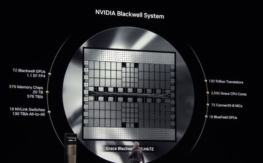
Blackwell Ultra (B300 Series)
Release Date: Second half of 2025
Overview: Blackwell Ultra is an enhanced version of the existing Blackwell architecture, serving as a mid-cycle refresh rather than a completely new design.
Specifications:
Memory: Up to 288 GB of HBM3e memory (an increase from 192 GB in the standard Blackwell B200).
Performance: Expected to deliver a 50% performance uplift over the B200 series, with a thermal design power (TDP) of approximately 1,400 watts.
Additional Features: Includes eight stacks of 12-Hi HBM3e memory and integration with Nvidia’s Mellanox Spectrum Ultra X800 Ethernet switch for improved data connectivity.
Rubin (Vera Rubin Platform)
Release Date: Second half of 2026
Overview: Rubin marks Nvidia’s next major architectural leap, designed to push the boundaries of AI and high-performance computing.
Specifications:
Memory: 288 GB of HBM4 memory, the next generation of high-bandwidth memory.
Performance: Delivers 50 petaflops of FP4 inference performance per chip. A full NVL144 rack configuration provides 3.6 exaflops of FP4 compute, which is 3.3 times higher than Blackwell Ultra.
CPU Integration: Paired with the “Vera” CPU, featuring 88 custom ARM cores and 176 threads, connected via a 1.8 TB/s NVLink interface.
Architecture: Expected to be fabricated on TSMC’s 3nm process, offering higher transistor density and improved power efficiency.
Rubin Ultra
Release Date: Second half of 2027
Overview: Rubin Ultra is an upgraded variant of the Rubin architecture, further boosting performance and capacity.
Specifications:
Memory: Up to 1 TB of HBM4e memory, a significant jump in capacity and bandwidth.
Performance: Provides 100 petaflops of FP4 compute per chip, achieving a 14x performance increase over the GB300 NVL72 platform.
Configuration: Utilizes the NVL576 rack configuration with four reticle-sized GPUs for maximum scalability.
Feynman Architecture
Release Date: 2028
Overview: Feynman is the next architecture in Nvidia’s pipeline following Rubin, though details remain limited at this stage.
Specifications:
Specific features are not yet fully disclosed, but it is expected to incorporate next-generation HBM memory (possibly HBM5 or beyond) and further advancements in AI compute capabilities.
As a future architecture, it will likely build on the Rubin platform’s innovations, targeting even higher performance for AI and general-purpose computing workloads.


Brian Wang is a Futurist Thought Leader and a popular Science blogger with 1 million readers per month. His blog Nextbigfuture.com is ranked #1 Science News Blog. It covers many disruptive technology and trends including Space, Robotics, Artificial Intelligence, Medicine, Anti-aging Biotechnology, and Nanotechnology.
Known for identifying cutting edge technologies, he is currently a Co-Founder of a startup and fundraiser for high potential early-stage companies. He is the Head of Research for Allocations for deep technology investments and an Angel Investor at Space Angels.
A frequent speaker at corporations, he has been a TEDx speaker, a Singularity University speaker and guest at numerous interviews for radio and podcasts. He is open to public speaking and advising engagements.


Related Posts


Stay Informed With the Latest & Most Important News
Previous Post
Next Post


Advertisement